This seemingly endless virus lock-down has freed up a lot of time to pursue long-dormant interests. I decided to look into VLF listening, which led to a search for an inexpensive receiver. I came across the NASA VLF-3, among others. After building one prototype from the schematics, I discovered a couple of annoyances. I cannot state with certainty that these issues are as objectionable in the NASA receiver kit, but I suspect that most are inherent in the design.
IMPORTANT: while this project is based on the NASA VLF-3 design, it is NOT sponsored, approved, or supported by NASA or any of their affiliates. The changes noted below are entirely my own.
I identified a couple of issues with the headphone amplifier. The first issue was the increase in background noise on the data channel as the headphone volume was increased. When the headphone amplifier was switched off, the noise was not present. A few minutes on the test bench with a scope indicated that the receiver would benefit from improved power supply decoupling and bypassing. I incorporated these changes in the revision 2.x boards.
The other issue was the background noise in the headphones at low volume levels. While this may not have been noticeable at high volume levels, once identified, I wanted to get rid of it. Research on the web suggests that this is a fairly common complaint with the LM386 and is also relatively easy to fix. Additional feedback from pin 5 to pin 8 with a series resistor and capacitor took care of this quite nicely.
Other changes to the published NASA design include the following:
- I moved the takeoff point for the headphone amplifier to the input of the data amplifier.
- I reduced the gain of the headphone amplifier to approximately 50 instead of 200.
- I added a connection for a loop antenna without having to hack into the board.
- I added a power jack to enable use of an external power source.
- I also added a jack to access the ‘second’ data channel.
- I added a 60 Hz notch filter and repurposed the data channel switch to be able to switch the notch filter out.
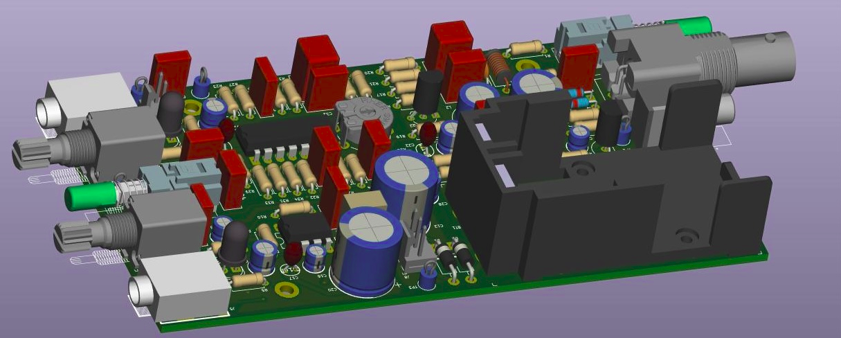
The receiver repackaging necessitated a new layout, with careful attention to the power and ground connections. I added power isolation and improved bypassing throughout.
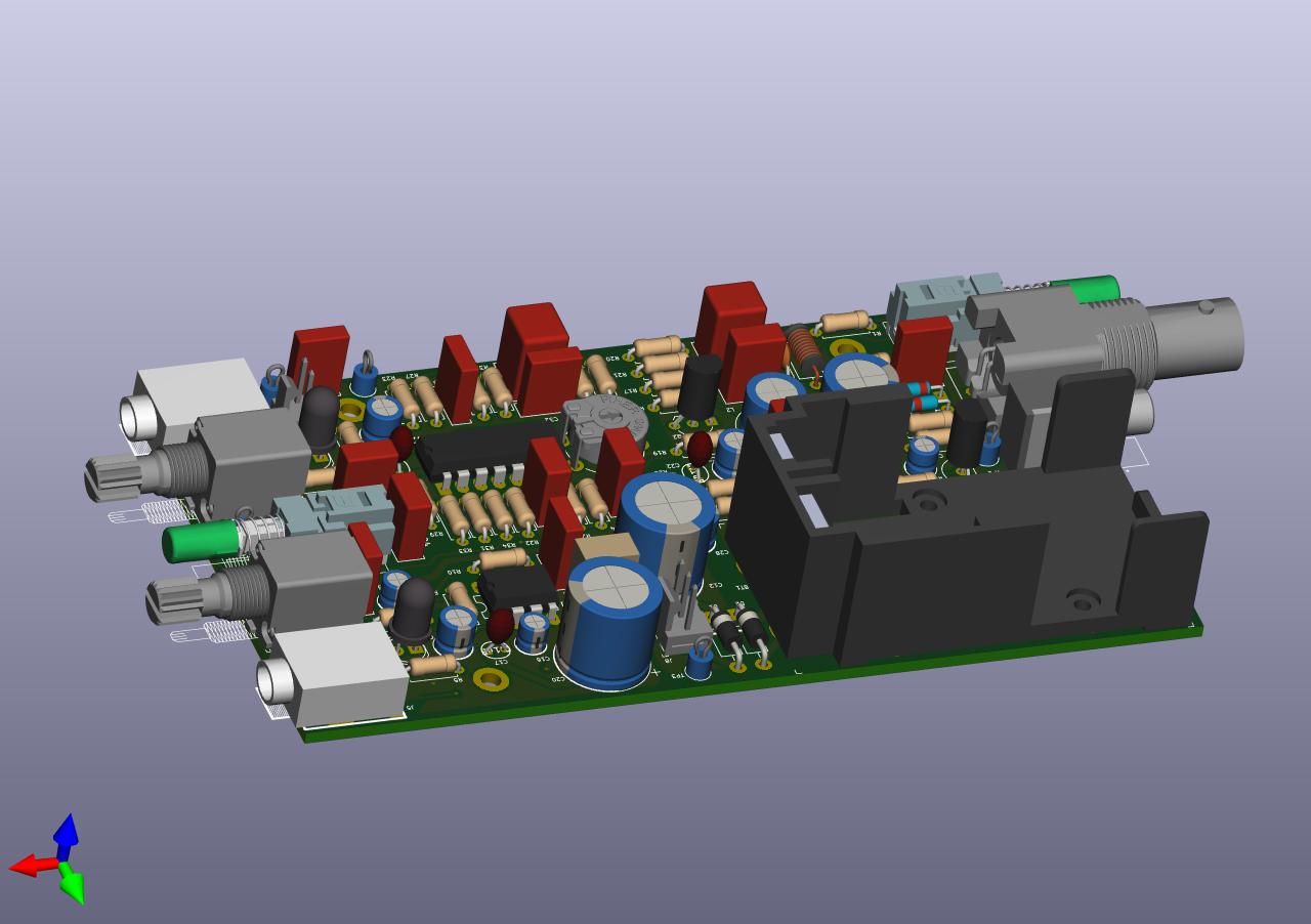 Internal electronic noise is an unavoidable byproduct of any electronic device, but it can be minimized by the careful selection of the proper components. At least two, and possible three of the active devices are becoming difficult to purchase from established primary vendors. Though some may be available from surplus and closeout channels, once those are gone, replacement with more current parts is the only option.
I selected a low-noise FET and transistor for the first two stages. Though not likely to impact the overall noise figure significantly, the op-amp is also a low-noise type. In addition, all resistors in the signal path are metal film.
I have just completed the rev 2.3 layout, sent it to production, and built the first example. All went as planned, except for one minor hiccup. Fortunately, the issue was easily correctable so a new spin of the board was not necessary. I corrected the gerbers, so the issue is not there on the files that are now available on OshPark. Current OshPark pricing is $65.00 for a set of three boards. I am also posting a complete set of files here and on GitHub. That way you can send the files to a board fabricator of your choosing.
The board is designed to fit into a Serpac A-27 enclosure, readily available from either Mouser or Digikey. All of the other components are available from these two suppliers, as well as several other major vendors.
Files necessary to duplicate this project are here:
References