The recent acquisition of one of the low cost VNAs led to this project. While the nanoVNA was originally purchased as an addition to my antenna test equipment, this little gadget is capable of so much more. Among its many capabilities, it enables me to accurately evaluate and select components for use in some transmitters and receivers I am interested in.
After hacking together a couple of quick and dirty fixtures, I felt the need to add a proper test fixture to my equipment. Consistent evaluation and comparison of components requires a consistent test environment. My quick hacks worked but not consistently. The test fixture frequently took so much effort that the project was pushed aside. After researching various designs on the web, I settled on this one as best fitting my budget and needs. I settled on the following requirements: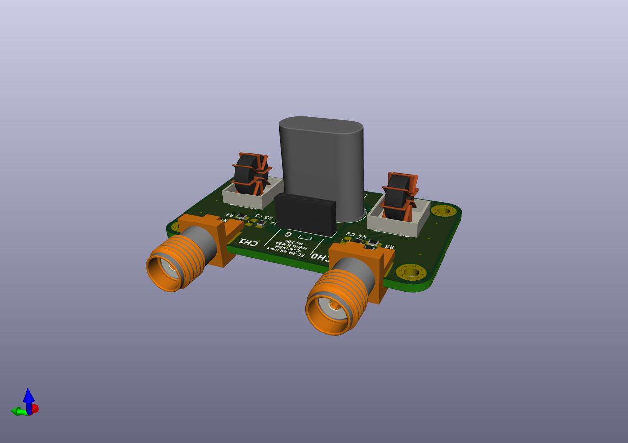
- Accommodates most small components
- Provide appropriate low impedance environment (12.5 ohms) for crystals
- Impedance transformation achieved by an attenuator, or by a transformer, or by a combination thereof
- Can be built with no attenuation or transformation
- Connector spacing to enable direct attachment to nanoVNA (with suitable connectors)
- Most leaded components can be plugged directly into test socket
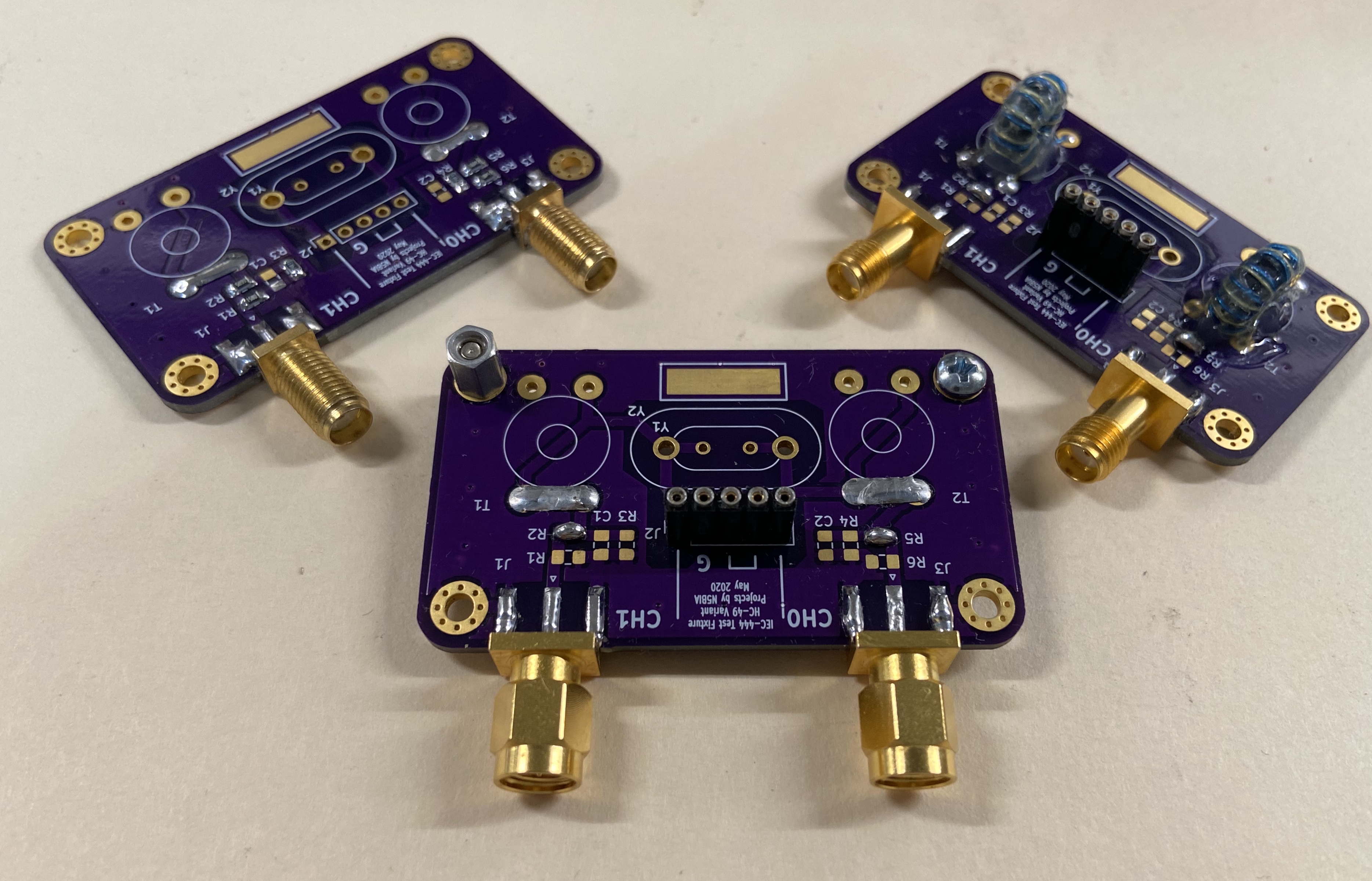
- HC33 and HC49 crystals can be plugged in with no soldering
- SMD crystals can be clamped by fashioning a suitable ground clamp
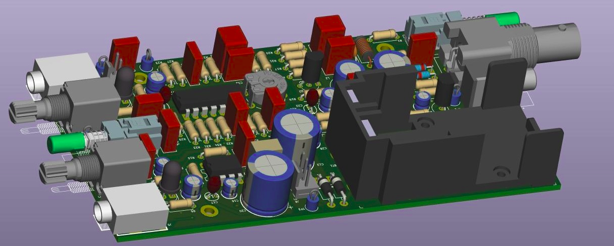
The schematic, component location diagram, and parts list are available here.
Boards
The design files (gerber files) are available on OSH Park as a shared design. The parts list is included on the schematic as well as here.
Assembly
Assembly requires a steady hand, good lighting, a small soldering tip, and probably a magnifier. A heat gun with a small outlet is also helpful. A suitable one can be found at most hobby stores that offer paper embossing supplies. A hot-melt glue gun is a handy accessory if you are building the transformer match version.
If you are building the transformer version, begin by winding the two matching transformers. Wind 10 bifilar turns on each core. The first pass through the core counts as #1. I found it easier to center the core on the wire, wind five turns in one direction, then wind the remaining turns in the other direction. Pull the wires tight and lay them neatly as you go. When you have the ten turns in place, a spot of hot-melt glue keeps the assembly neat.
The attenuator resistors are all 0805 surface mount. Not too difficult, even for these 70+ year old eyes. Begin with the resistors. I tacked one end of each in position, then tacked the other end. Use the heat gun to apply heat to the entire resistor area while -gently- tapping on a corner of the board. When the solder melts, the resistors will center themselves on the pads because of the surface tension of the molten solder. Stop tapping, remove the heat, and let the solder cool. See, that wasn't to bad...
Install any sockets you plan to use. This is a 'DIY' option, best determined by how you plan to use the adapter. As inexpensive as these are to build, I suggest making a couple of different styles. Next up, install the transformers or the jumpers to bypass them.
Calibration
The last item is the input/output connectors. The sites for these connectors are spaced to enable a direct connection to the nanoVNA if you want. If you are going to build them this way, first attach the connectors to the VNA, then align and insert the board into the connector bosses. Carefully solder the center conductor only, then remove the adapter from the VNA. Solder the ground sides of the connector, top and bottom.
All done! Clean the flux residue from the board, carefully inspect the solder joints. Re-flow any that appear suspect.
Before beginning measurements, a standard SOLT calibration for the frequency of interest is essential. Select the nominal center frequency for the crystals being examined. Set the span to cover 50kHz to 100kHz either side of the nominal crystal frequency to perform the calibration.
Measurement
Measurement technique depends on the software you will use to perform the measurements. I have only the nanoVNA at present, so the following discussion is somewhat limited as to details. The general concepts, as I understand them now, are applicable.
The first task is to perform the calibration as described previously. If you are connecting the test fixture directly to the nanoVNA, perform the SOLT procedure for the frequency span of interest and save it in one of the memories.Remember, you have only 100 calibration points in a sweep, use them wisely. You will need to sweep more than 50 Hz when you begin drilling down on the crystal you are examining. You can use nanoVNA Saver to perform the calibration and save a calibration file to be loaded later if your software has this feature. Otherwise, you will need to use an internal calibration with points spaced at 5 to 10 Hz. In practice, I doubt that this is a serious issue.
I have found several software tools to perform and record crystal parameter measurement. These are written with Python, which should make them workable across all three major operating systems. These are available for download from github.
amcp - automated measurement of crystal parameters - https://github.com/Battosai42
crystalweb - automated crystal measuerment - https://github.com/roseengineering/crystalweb
nanoVNA saver - general purpose VNA control and measurement - https://github.com/mihtjel/nanovna-saver
Bibliography
References and resources I used while developing this project:
- www.warc.org.uk Ladder Crystal Filters For Radio Amateurs -- Jack Hardcastle, G3JIR
- q2gxo.wordpress.com/2010/04/05/crystal-ladder-filters-i-software/ Crystal ladder filters - Software - Dishal by DJ6EV
- Crystal Ladder Filters for All QEX - Horst Steder, DJ6EV and Jack A. Hardcastle, G3JIR - Nov/Dec 2009
- http://www.hamcom.dk/VNWA/Crystal Test Fixture for DG8SAQ VNWA and N2PK VNA.pdf
- https://github.com/mihtjel/nanovna-saver
- https://github.com/Battosai42
- https://github.com/roseengineering/crystalweb
- https://groups.io/g/nanovna-users
- https://groups.io/g/PHSNA
NOTE: some references listed above have expired SSL certificates. While I do not believe they indicate malicious attempts, in an abundance of caution and in the interest of completeness, I am including the reference and leaving it to you, the reader, to decide how you wish to proceed.